The J-Link debugger sold by Segger is a debugger probe for ARM Cortex-M processors like the ones sold by ST, Microchip, Nordic Semiconductor, Texas Instruments, Silicon Labss and many others. It’s one of the most popular debug probes available, and it’s a fantastic too for reverse engineering and firmware extraction and analysis.
J-Link debuggers have very wide chipset support and IDE support. You can reverse and develop new firmware if you need.
We’ve used a lot of debug probes, including some cheap Chinese ones. Even though you’ll save some money, the long term hassle in dealing with their lack of support is usually not worth it.
Picking a J-Link
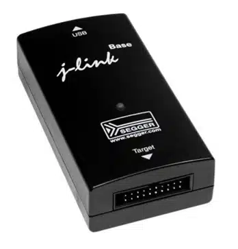
For a long time, the J-Link debug adapter was relatively large and looked like this.
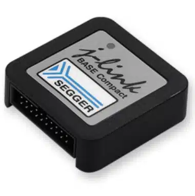
Some time ago Segger released a compact line of debuggers that are smaller and have the same functionality. Although it doesn’t really make a huge difference, a compact design makes life easier when going to an on-site assessment to work on devices.
Notice how the two say “Base”? Segger has several versions of their debugger. The pro versions allow for more hardware breakpoints among other things. We rarely need to use anything but the Base version, especially since the others can get close to $1k per unit.
Segger J-Link Utilities
One of the great things about the J-Link debuggers is the software support, with a mature and quite stable software.
The first thing you need to do is to install the J-Link software which are all the drivers and software you need. You can download the software from here: https://www.segger.com/downloads/jlink/
A computer can usually have multiple versions of the J-Link software at the same time, but if there are issues you should uninstall older versions.
The J-Link software installs a lot of utilities. Let’s cover the important ones
- J-Link RTT Viewer – Think of RTT as a printf that goes across the debugger and is fast. Developers sometimes leave RTT enabled in their device, letting you capture a bunch of debug information that can be critical
- J-Link Commander – This is the J-Link Swiss knife that allows you to run a whole slew of commands like reading and writing memory, flash and registers
- J-Flash Lite – A quick utility for programming firmware to devices without having to use command line
Getting Access to JTAG and SWD
To use J-Link, you first need to find the pads or contacts on the board. Those signals depend on the design itself, and every design is unique. But there are in general two main protocols for Cortex-M devices.
SWD is a low pin count version of JTAG that many microcontrollers and products use. The other protocol is JTAG which is also very common. How do you know which one to use? You will need to check the pinout of the device. Typically these signals are brough out to a header or contact points that allow programming the system in production.
JTAG and SWD Pinout Signals
| JTAG Signal |
| TDO |
| TDI |
| TMS |
| TCK |
| RST |
| GND |
| VCC |
| SWD Signal |
| SWD |
| SCLK |
| RST |
| GND |
Note that for SWD the RST line is often optional and not mandatory, but with it you can make sure the system is in the right spot. In some cases you actually want to avoid connecting RST because you want to avoid resetting the processor.
The interface speed is by default 1000kHz, which is OK. But depending on the device and the connections, you can go faster. If you have a relatively short connector between the Segger J-link, with good grounding, you should be able to go 4000kHz (4MHz).
What do I mean? If you connect Segger using a a short ribbon cable connector, then there will be plenty of ground pins that will help maintain good signal integrity to your target. But if you are using single wires, then the ground may be far away, and then you’ll see weird errors happen sometimes.
If you’re seeing errors, it’s a good idea to lower the speed to 1000kHz or even 500kHz to see if they go away. If they do, then it’s time to improve the connection. You don’t want to get errors when cloning the firmware.
J-Link RTT Viewer
As I mentioned before, RTT viewer is the client side utility for receiving RTT logs across the debugger.
For devices you’re reverse engineering, RTT has to be enabled and used by the device. This can sometimes happen when developers forget to disable it, or leave it in release modes of the firmware. This can be a huge boon for reverse engineering the firmware since these prints can provide a lot of information about what’s happening.
But RTT isn’t just printf. RTT also allows for you to send commands to the device if that’s a feature that’s been enable. I’d say it’s a lot less common than the outgoing prints, but it can happen.
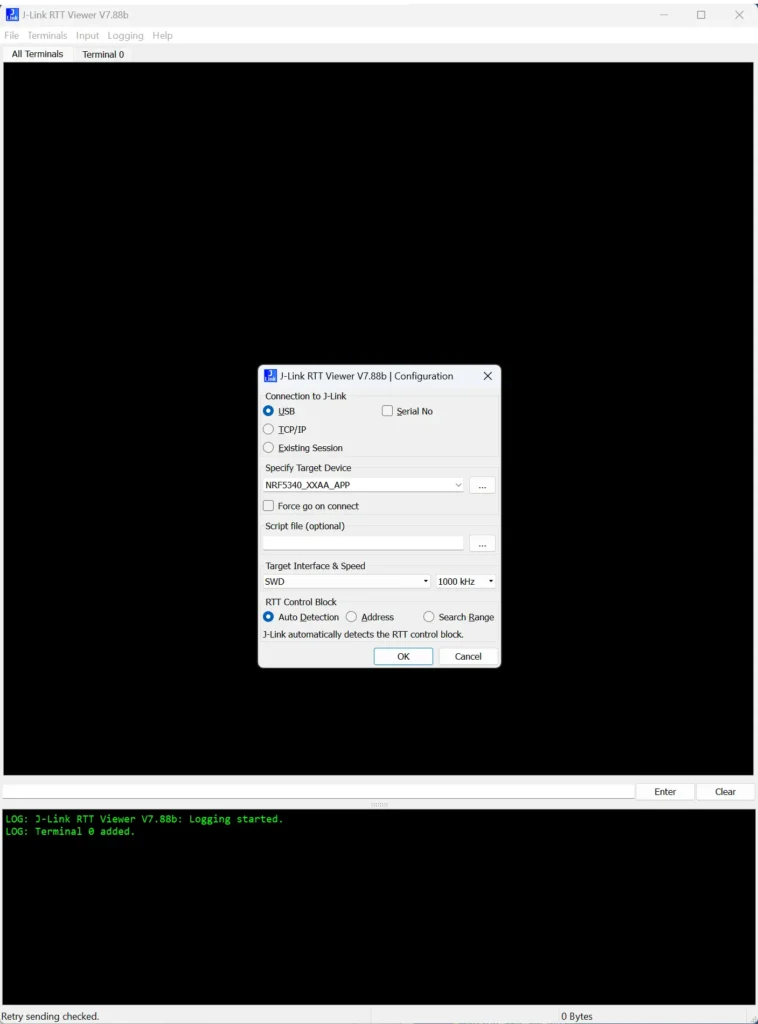
When you start RTT Viewer, this is the screen you’ll see. The most critical item here is to pick the right debugger and the right target.
If you have only one debugger connected to the computer via USB, especially on Windows, you won’t need to do anything. If you have multiple debuggers you can select the one you want specifically by its Serial Number, which is usually a sticker on the back
If you have a J-Link with Ethernet, you can specify the IP address and connect to it that way. Usually there’s no need to do anything more if you just have one debugger.
Now, selecting the Target Device is critical, because every device has different capabilities, memory space, etc.
How do you know which device to use? When you’re reverse engineering a system you’ll typically need to look at the chip markings. They’ll tell you the vendor and the part number.
If the markings on the microcontroller have been removed or can’t be retrieved, then it’s possible to find it in other ways. The package of the microcontroller pinout, etc. can all give you hints about what the part number is.
Assuming you know the part number, you can click on the … button and select the exact part #
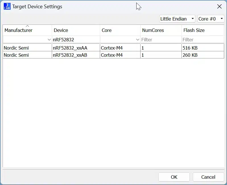
You can see that I’ve filtered on the nRF52832, and there are two variants. The difference between them is the flash size, which is pretty important if we want to later read the flash.
With the right variant selected we press OK.
Back at the main screen there’s a couple extra options:
Target Interface & Speed
The two main interfaces you’ll use are SWD and JTAG. For TI devices, cJTAG is also possible.
RTT Control Block
The RTT control block is a special section of memory (RAM) that contains the RTT information and the data being transferred. You need to know where this block is located in order to read the data from it. Every application defines the location of the RTT control block in a different location. It can even change when compiling because the linker can shift the address.
Luckily, the control block has some special patterns in it that allows the RTT client to find it easily, so in most cases the auto detection works.
Capturing RTT
Once you’re all configured, you can just press OK on the main screen. The RTT Viewer will try and find the RTT control block. If it does, it will automatically begin streaming any prints.
If RTT doesn’t detect any control block, it’s likely whatever firmware is running on your device doesn’t have RTT capability enabled.
J-Link Commander
The real meat and potatoes here is J-Link commander, a utility that lets you control the processor, access memory and registers. It’s an interactive console program where you can type commands.
Now, to make things easier, we’re going to run J-Link commander from a user folder.
Open Command Line, CD to a folder, and then type the command
J-Link>"C:\Program Files\SEGGER\JLink\JLink.exe"Once this runs, you will see the following along with the commands I ran to connect to the device
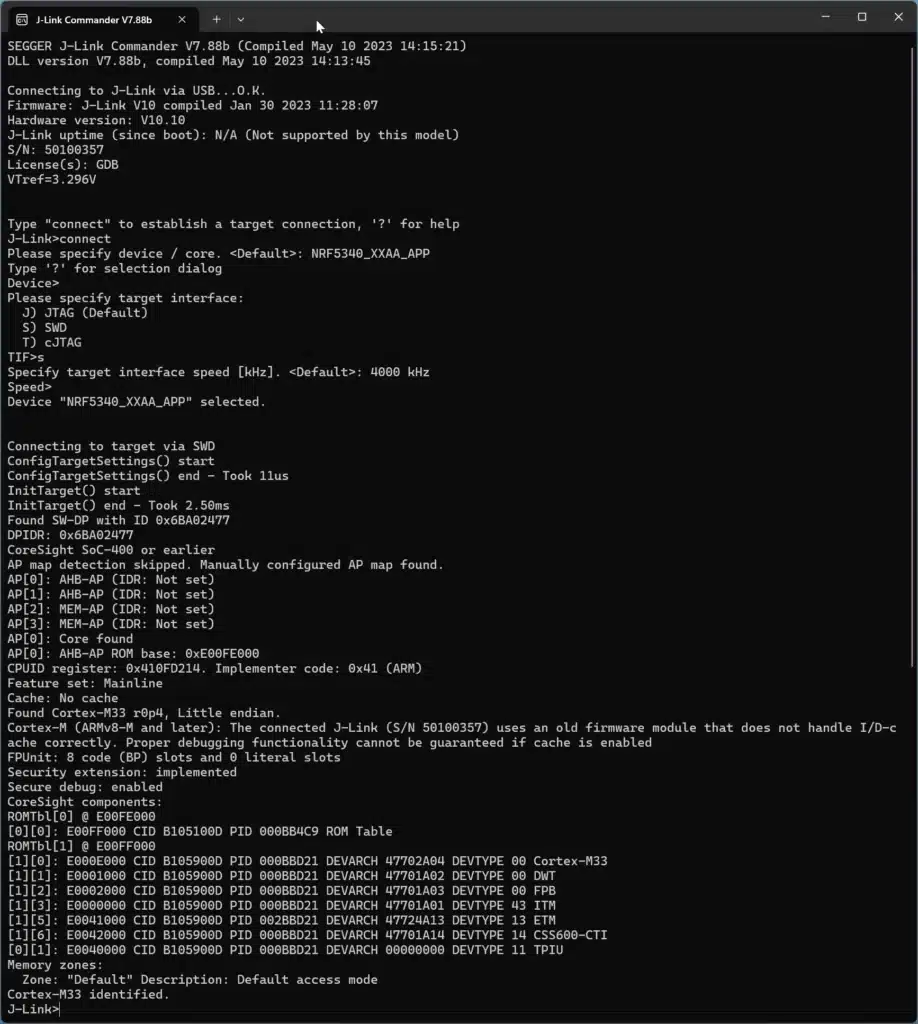
Above you will see the screen. Notice that when you first start the screen you’re told to type connect to start a connection, then you choose a CPU, an interface (SWD in this case) and speed. This is similar to the RTT viewer.
You can see that after we selected these options the console prints “Connecting to target via SWD”. It successfully detects the Cortex-M33 core along with other components in the device.
Commands
You can see what commands are available by typing ? and pressing ENTER. You will get every single command available. We’re going to focus on the most useful commands.
Controlling the CPU
When we’re connected, the CPU may still be running. We can stop the CPU from running using the halt command:
J-Link>halt
PC = 00000DB8, CycleCnt = 00000000
R0 = 00000000, R1 = 00000000, R2 = 00000000, R3 = 00000000
R4 = 00000000, R5 = 00000000, R6 = 00000000, R7 = 00000000
R8 = FFFFFFFF, R9 = FFFFFFFF, R10= FFFFFFFF, R11= FFFFFFFF
R12= FFFFFFFF
SP(R13)= 20000BF8, MSP= 20000BF8, PSP= 00000000, R14(LR) = FFFFFFFF
XPSR = F9000000: APSR = NZCVQ, EPSR = 01000000, IPSR = 000 (NoException)
CFBP = 00000000, CONTROL = 00, FAULTMASK = 00, BASEPRI = 00, PRIMASK = 00
MSPLIM = 00000000
PSPLIM = 00000000

Security extension regs:
MSP_S = 20000BF8, MSP_NS = 00000000
MSPLIM_S = 00000000, MSPLIM_NS = 00000000
PSP_S = 00000000, PSP_NS = FFFFFFFC
PSPLIM_S = 00000000, PSPLIM_NS = 00000000
CONTROL_S  = 00, FAULTMASK_S  = 00, BASEPRI_S  = 00, PRIMASK_S  = 00
CONTROL_NS = 00, FAULTMASK_NS = 00, BASEPRI_NS = 00, PRIMASK_NS = 00

FPS0 = 00000000, FPS1 = 00000000, FPS2 = 00000000, FPS3 = 00000000
FPS4 = 00000000, FPS5 = 00000000, FPS6 = 00000000, FPS7 = 00000000
FPS8 = 00000000, FPS9 = 00000000, FPS10= 00000000, FPS11= 00000000
FPS12= 00000000, FPS13= 00000000, FPS14= 00000000, FPS15= 00000000
FPS16= 00000000, FPS17= 00000000, FPS18= 00000000, FPS19= 00000000
FPS20= 00000000, FPS21= 00000000, FPS22= 00000000, FPS23= 00000000
FPS24= 00000000, FPS25= 00000000, FPS26= 00000000, FPS27= 00000000
FPS28= 00000000, FPS29= 00000000, FPS30= 00000000, FPS31= 00000000
FPSCR= 00000000
J-Link>
In many cases J-Link will stop the CPU automatically for certain commands. We can start the CPU again with the Go command:
J-Link>Go
J-Link>
We can also reset the device, causing the CPU to restart:
J-Link>reset
Reset delay: 0 ms
Reset type NORMAL: Resets core & peripherals via SYSRESETREQ & VECTRESET bit.
Reset: ARMv8M core with Security Extension enabled detected.
Reset: Halt core after reset via DEMCR.VC_CORERESET.
Reset: Reset device via AIRCR.SYSRESETREQ.
Downloading Flash Firmware
Since we’re connected to the CPU we can now read the flash memory. Flash is where the code of the device is stored. While every device is different, the nRF5340 we’re debugging has 1MB of Flash and 512kB of RAM. Since the device is a Cortex-M, then the addresses start at 0x00000000. However, you should always check the datasheet of the device because sometimes ROM can be located at that address.
Looking at the nRF5340 memory map we can see:
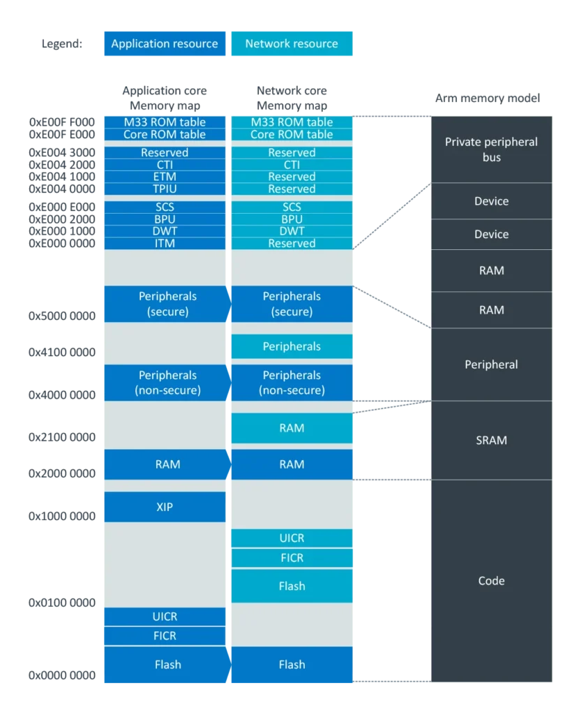
The nRF5340 has two CPU cores, but we’re connected to and are interested in the Application Processor.
We can see that Flash starts at 0x0000 0000 and including the FICR and UICR extends to 0x0100 0000.
Because Flash is 1MB, we can assume that its length is 0x100000 or 1,048,576 bytes. So let’s grab that
J-Link>savebin output.bin 0x0 0x100000
Opening binary file for writing... [output.bin]
Reading 1048576 bytes from addr 0x00000000 into file...O.K.
J-Link>
output.hex will be created in the the current working folder
Understanding BIN and HEX files
When downloading firmware from devices you’ll often deal with bin and hex files. The difference is that a bin file is raw binary bytes of data. When you have a binary file, you don’t know where they belong or came from. There is no address information
Hex files on the other hand contain exact addresses.
When programming binary files, you will need to provide a base address that will be used. When you use hex the address information is already there.
Hex files have another advantage which is that they can contain multiple non-contiguous sections. Part of the Hex file format is the ability to specify start addresses.
Downloading Memory
RAM can be extremely useful when analyzing a device, because it can contain passwords, keys and useful information about variables. You can bypass and change the running device state. Using J-Link we can read all of RAM as well.
Since RAM is memory mapped, we can download it similar to
J-Link>savebin ram.bin 0x20000000 0x40000
Opening binary file for writing... [ram.bin]
Reading 262144 bytes from addr 0x20000000 into file...O.K.
J-Link>
Now we have a copy of all the device RAM at the current state.
What’s the usefulness? We capture the state of a device at a certain point in time. We can restore the device, or compare the behavior of the device by comparing the memory, seeing how it changes.
Loading Flash and Memory
We’ve captured the firmware and flash, but we often need to program the device as well.
J-Link>loadbin output.bin 0x0
'loadbin': Performing implicit reset & halt of MCU.
Reset: ARMv8M core with Security Extension enabled detected.
Reset: Halt core after reset via DEMCR.VC_CORERESET.
Reset: Reset device via AIRCR.SYSRESETREQ.
Downloading file [output.bin]...
J-Link: Flash download: Bank 2 @ 0x00000000: Skipped. Contents already match
O.K.
J-Link>
In this case we already have the same data in Flash, so the download is skipped since J-Link compares the contents.